

高等学校化学学报 ›› 2025, Vol. 46 ›› Issue (2): 20240380.doi: 10.7503/cjcu20240380
温俊青1( ), 王嘉辉1, 张建民2
收稿日期:2024-08-05
出版日期:2025-02-10
发布日期:2024-10-28
通讯作者:
温俊青
E-mail:wenjq2013@163.com
基金资助:
WEN Junqing1(), WANG Jiahui1, ZHANG Jianmin2
Received:2024-08-05
Online:2025-02-10
Published:2024-10-28
Contact:
WEN Junqing
E-mail:wenjq2013@163.com
Supported by:摘要:
采用第一性原理计算方法研究了C, Pd元素掺杂及点缺陷MoS2/ZnO异质结的电子结构、 光学性质及光催化性能. 计算结果表明, 本征MoS2/ZnO异质结具有0.66 eV的直接带隙, 带边位置呈现Ⅱ型能带排列. 掺杂和缺陷可以有效减小MoS2/ZnO异质结的带隙, Pd@Zn为磁性半导体, VMo和VZn体系具有磁性半金属特性. 掺杂和缺陷使MoS2/ZnO异质结禁带之中出现杂质能级, 有利于电子跃迁, 吸收范围扩展至红外波段, 在可见光范围(500~760 nm)内的光吸收系数提高. 本征、 掺杂与缺陷MoS2/ZnO异质结体系界面处均存在由ZnO层指向MoS2层的内建电场, 促使本征MoS2/ZnO异质结, C@S2, Pd@Zn, VS1, VS2和VO体系形成直接Z型异质结, 促进了光生电子-空穴对的有效分离. 异质结的带边电位跨过pH=0和7时的氧化还原电位, 表明这些异质结可以在强酸溶液与中性溶液条件下进行氧化还原反应, 且载流子具有较强的氧化还原能力. 研究结果为基于MoS2/ZnO异质结的设计提供了理论参考.
中图分类号:
TrendMD:
温俊青, 王嘉辉, 张建民. 掺杂和点缺陷调控MoS2/ZnO异质结光解水性能的第一性原理研究. 高等学校化学学报, 2025, 46(2): 20240380.
WEN Junqing, WANG Jiahui, ZHANG Jianmin. First-principles Study of Doping and Point Defects Modulating the Photodissociative Water Properties of MoS2/ZnO Heterojunction. Chem. J. Chinese Universities, 2025, 46(2): 20240380.
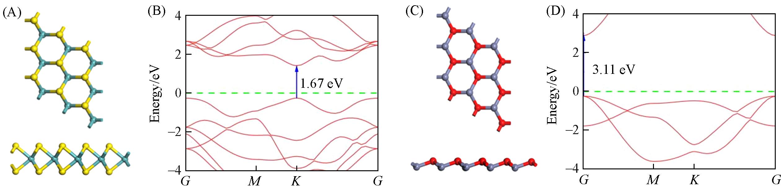
Fig.1 Top and side views of MoS2 mono⁃layer structure(A) and ZnO(001) structure(C), energy bands of MoS2 mono⁃layer(B) and ZnO(001)(D)Yellow stands for S atoms, cyan stands for Mo atoms, gray for Zn atoms, and red color represents O atoms.
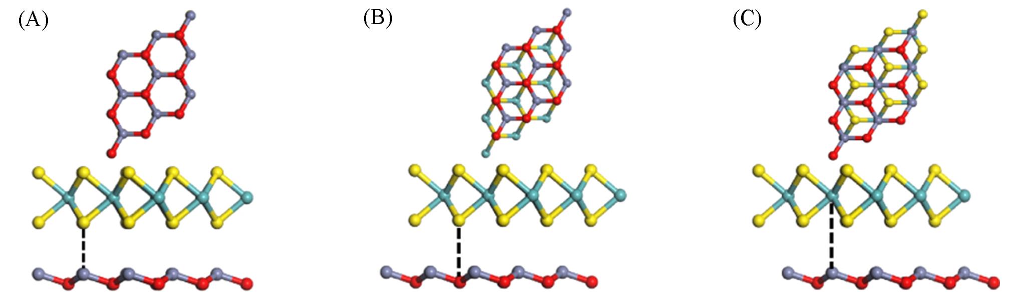
Fig.2 Stacking structures of AA(A), AB⁃Zn(B) and AB⁃O(C)
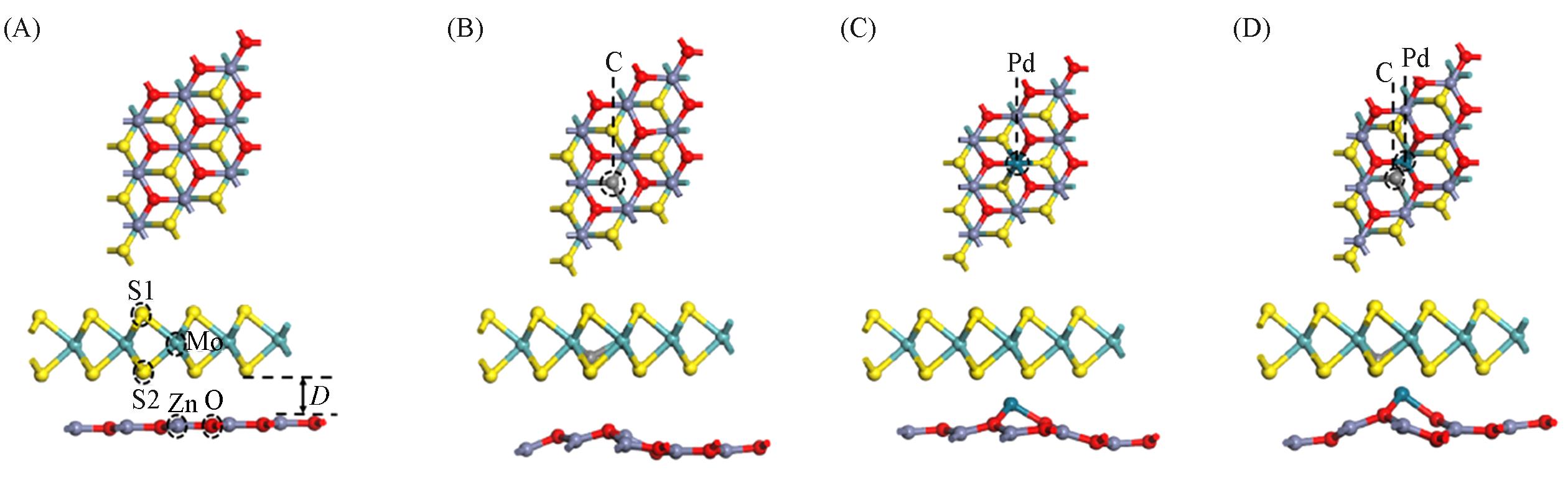
Fig.3 Doping stabilized structures of MoS2/ZnO(A), C@S2(B), Pd@Zn(C) and C@S2&Pd@Zn(D)
| Structure | Ef /eV | Structure | Ef /eV |
|---|---|---|---|
| C@S1 | 5.31 | VMo | 6.56 |
| C@S2 | 5.24 | VS1 | 3.50 |
| C@O | 9.59 | VS2 | 3.45 |
| Pd@Mo | 4.54 | VO | 4.94 |
| Pd@Zn | -6.49 | VZn | 2.92 |
| C@S2&Pd@Zn | 5.69 |
Table 1 Comparison of the Ef of different systems
| Structure | Ef /eV | Structure | Ef /eV |
|---|---|---|---|
| C@S1 | 5.31 | VMo | 6.56 |
| C@S2 | 5.24 | VS1 | 3.50 |
| C@O | 9.59 | VS2 | 3.45 |
| Pd@Mo | 4.54 | VO | 4.94 |
| Pd@Zn | -6.49 | VZn | 2.92 |
| C@S2&Pd@Zn | 5.69 |
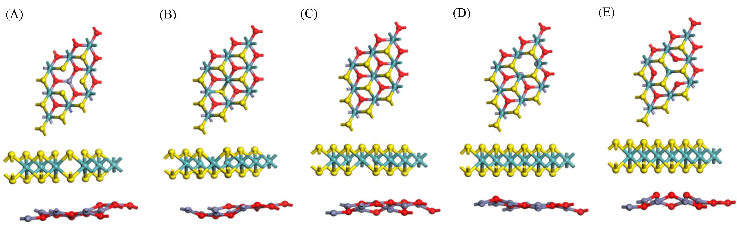
Fig.4 Structures of monatomic defects of VMo(A), VS1(B), VS2(C), VO(D) and VZn(E)
| Structure | D/nm | dMo—S/nm | dZn—O/nm | dC—Mo/nm | dPd—O/nm | 1023M/(A·m2) |
|---|---|---|---|---|---|---|
| MoS2/ZnO | 0.319 | 0.241 | 0.183 | — | — | 0 |
| C@S2 | 0.364 | 0.242 | 0.187 | 0.202 | — | 0 |
| Pd@Zn | 0.251 | 0.242 | 0.194 | — | 0.211 | 1.681 |
| C@S2&Pd@Zn | 0.212 | 0.241 | 0.188 | 0.214 | 0.221 | 0 |
| VMo | 0.430 | 0.240 | 0.187 | — | — | 1.418 |
| VS1 | 0.411 | 0.240 | 0.189 | — | — | 0 |
| VS2 | 0.409 | 0.239 | 0.187 | — | — | 0 |
| VO | 0.375 | 0.241 | 0.190 | — | — | 0 |
| VZn | 0.361 | 0.241 | 0.187 | — | — | 1.648 |
Table 2 Layer spacing(D), bond length(d) and magnetic moment(M) of MoS2/ZnO, doping and defective systems
| Structure | D/nm | dMo—S/nm | dZn—O/nm | dC—Mo/nm | dPd—O/nm | 1023M/(A·m2) |
|---|---|---|---|---|---|---|
| MoS2/ZnO | 0.319 | 0.241 | 0.183 | — | — | 0 |
| C@S2 | 0.364 | 0.242 | 0.187 | 0.202 | — | 0 |
| Pd@Zn | 0.251 | 0.242 | 0.194 | — | 0.211 | 1.681 |
| C@S2&Pd@Zn | 0.212 | 0.241 | 0.188 | 0.214 | 0.221 | 0 |
| VMo | 0.430 | 0.240 | 0.187 | — | — | 1.418 |
| VS1 | 0.411 | 0.240 | 0.189 | — | — | 0 |
| VS2 | 0.409 | 0.239 | 0.187 | — | — | 0 |
| VO | 0.375 | 0.241 | 0.190 | — | — | 0 |
| VZn | 0.361 | 0.241 | 0.187 | — | — | 1.648 |
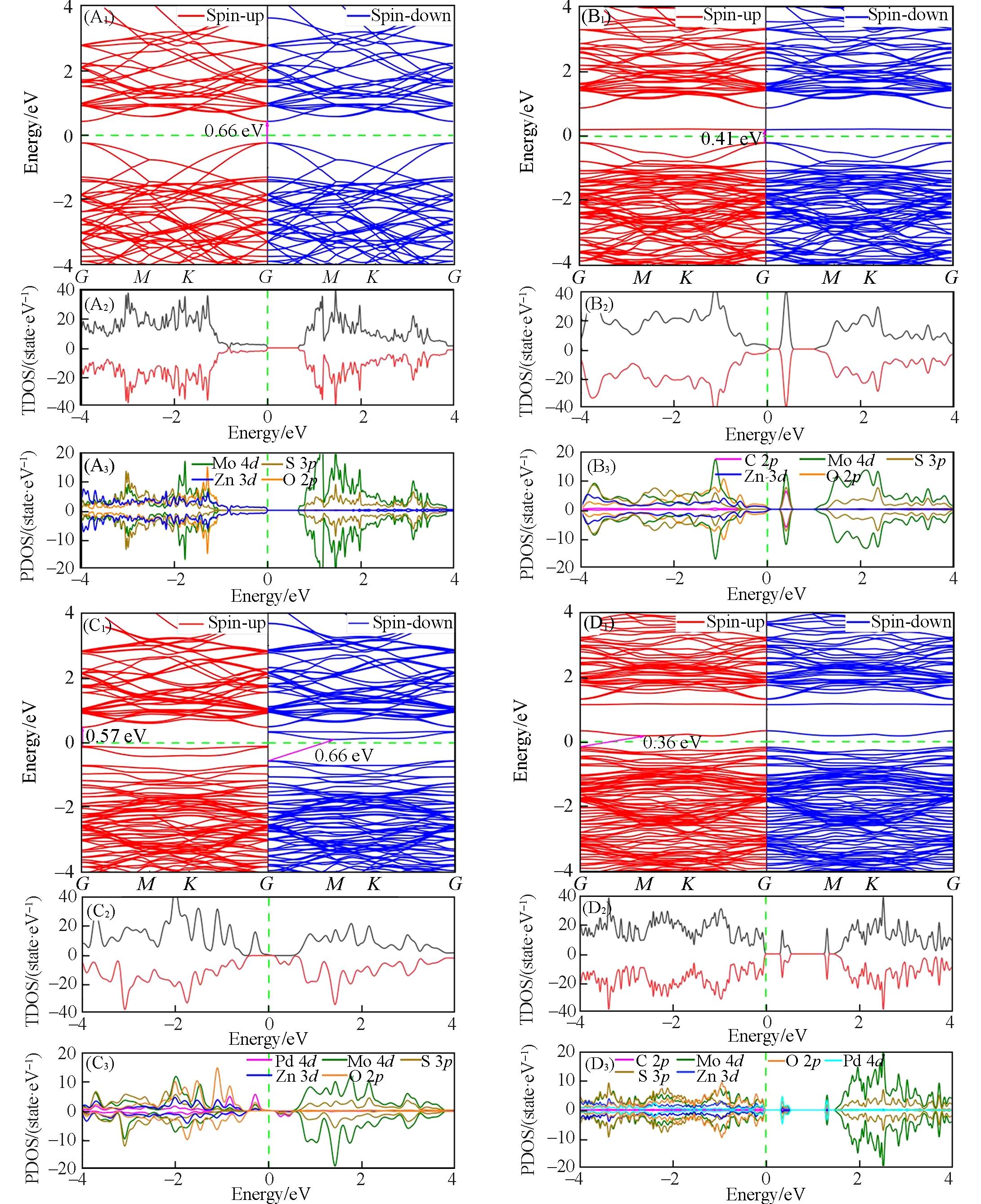
Fig.5 Band structures and density of states of MoS2/ZnO(A1—A3), C@S2(B1—B3), Pd@Zn(C1—C3) and C@S2&Pd@Zn(D1—D3)
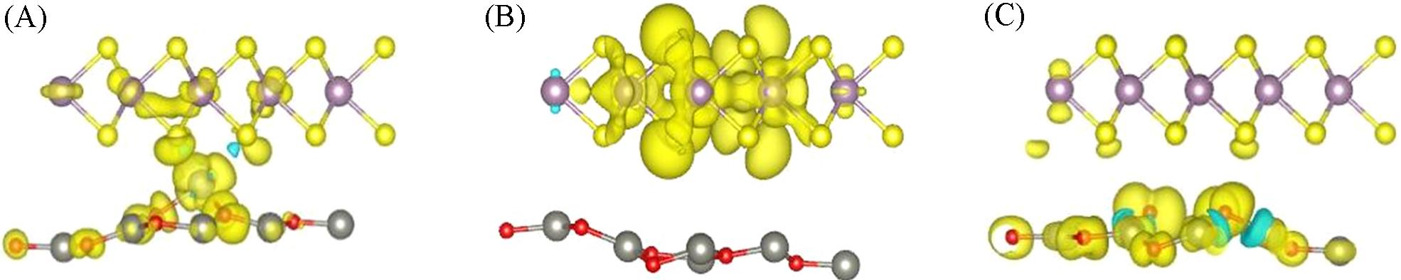
Fig.6 Spin charge density diagrams of Pd@Zn(A), VMo(B) and VZn(C)
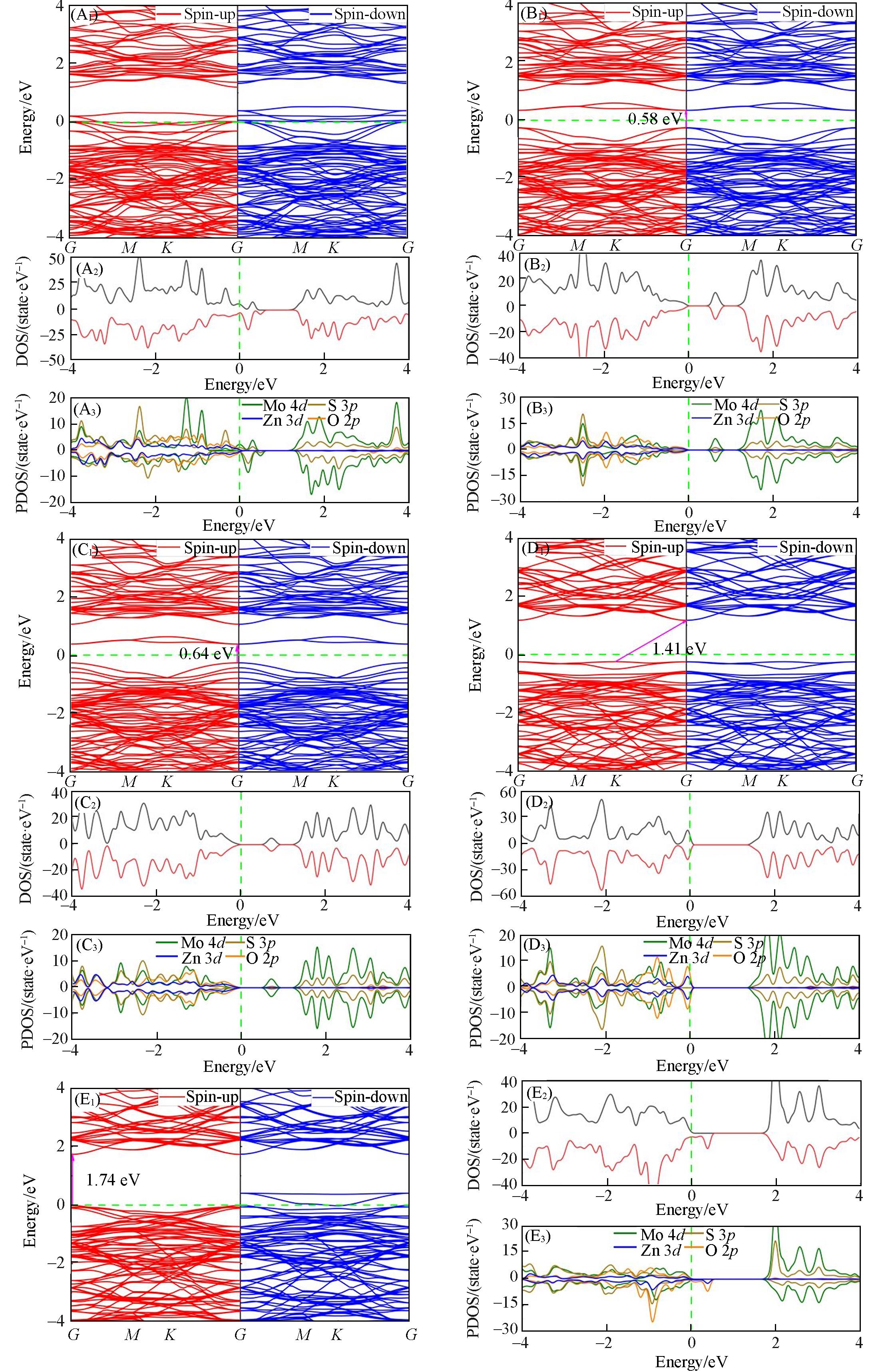
Fig.7 Band structures and density of states of VMo(A1—A3), VS1(B1—B3), VS2(C1—C3), VO(D1—D3) and VZn(E1—E3)
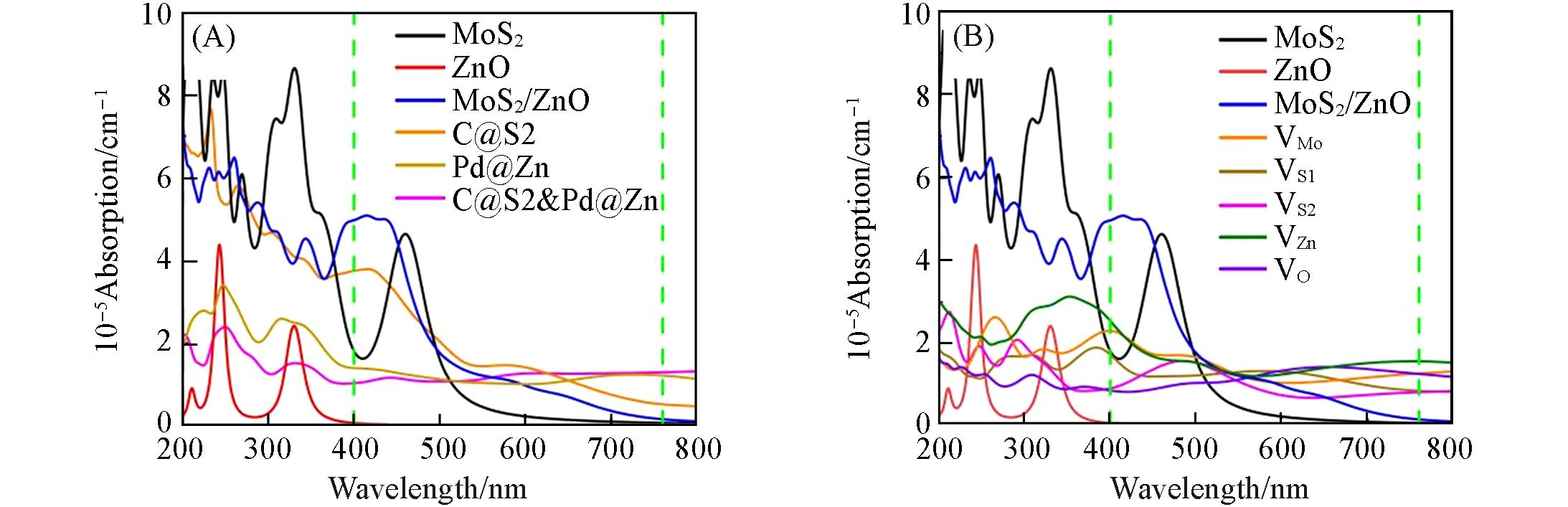
Fig.8 Optical absorption spectra of doping systems(A) and defective systems(B)
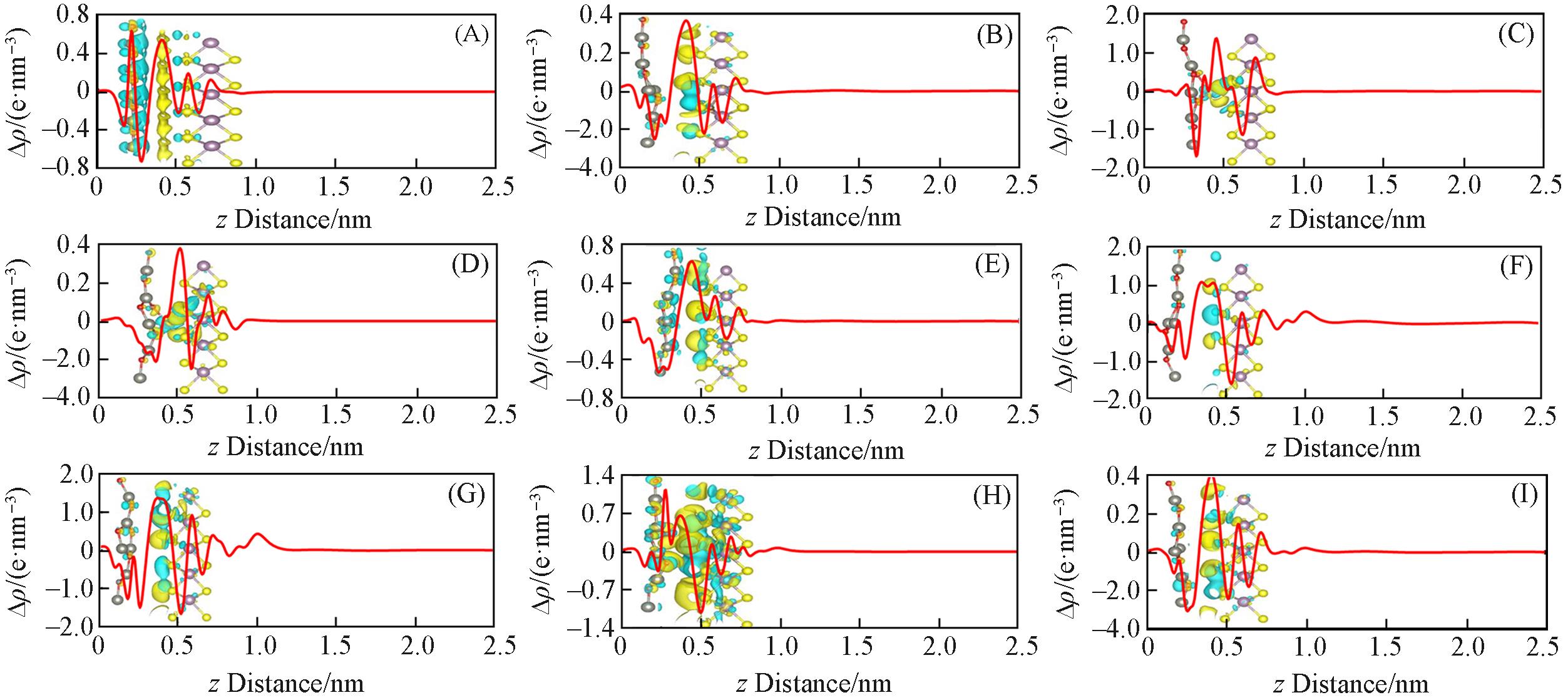
Fig.9 2D planar mean differential charge density(Δρ) of MoS2/ZnO(A), C@S2(B), Pd@Zn(C), C@S2&Pd@Zn(D), VMo(E), VS1(F), VS2(G), VZn(H) and VO(I)
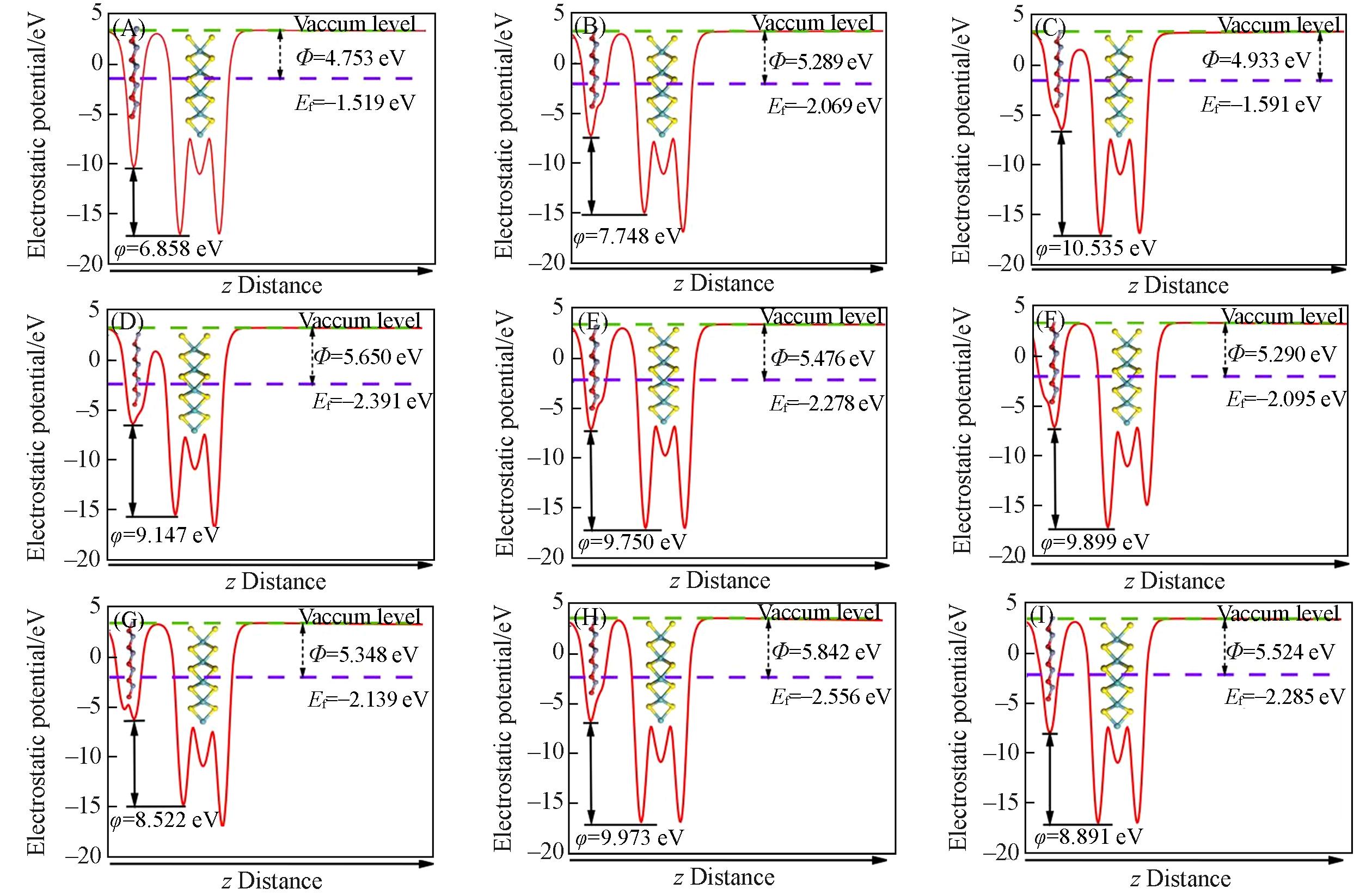
Fig.10 Work function of MoS2/ZnO(A), C@S2(B), Pd@Zn(C), C@S2&Pd@Zn(D), VMo(E), VS1(F), VS2(G), VZn(H) and VO(I)φ: The electrostatic potential difference.
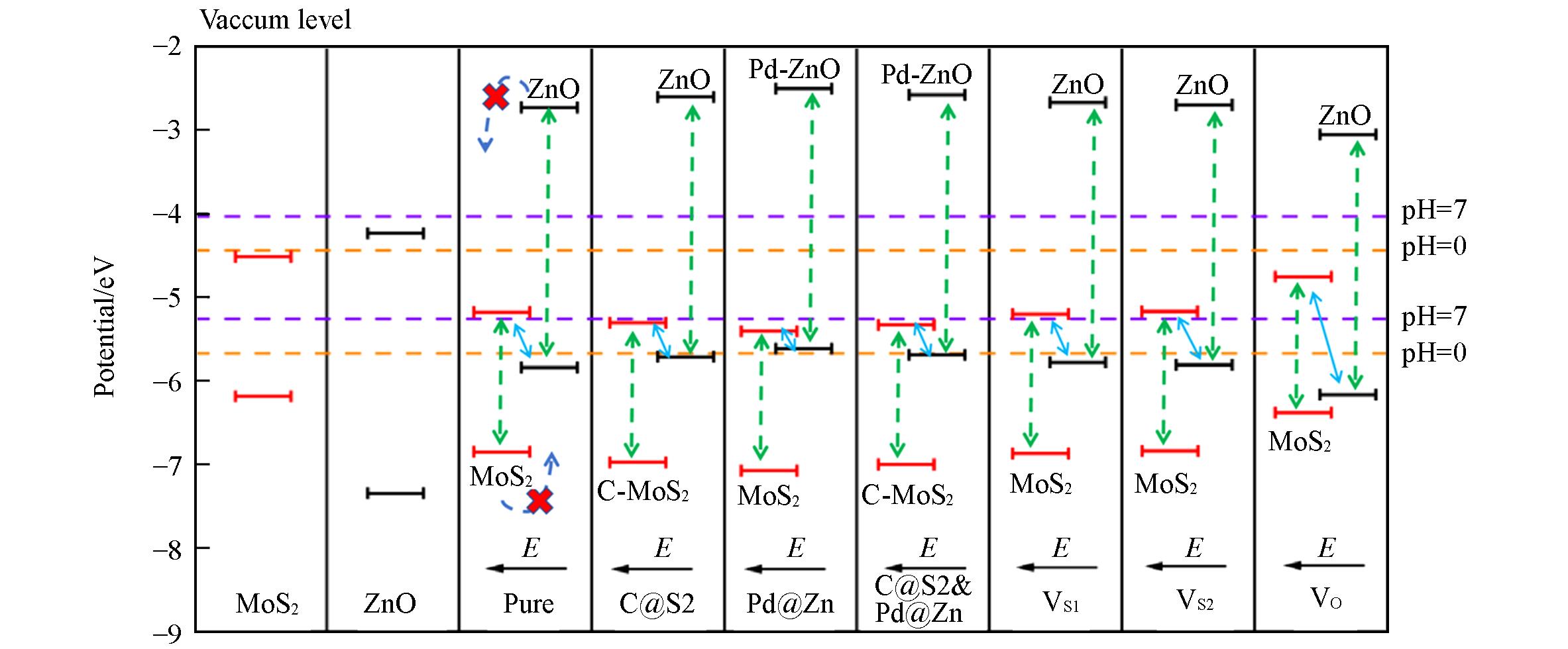
Fig.11 Band edge position of MoS2/ZnO, C@S2, Pd@Zn, C@S2&Pd@Zn, VS1, VS2 and VO
| 1 | Wickramaratne D., Zahid F., Lake R. K., J. Chem. Phys., 2014, 140(12), 124710 |
| 2 | Cai Y., Zhang G., Zhang Y. W., J. Am. Chem. Soc., 2014, 136(17), 6269—6275 |
| 3 | Cai Y., Lan J., Zhang G., Zhang Y. W., Phys. Rev. B, 2014, 89, 035438 |
| 4 | Amani M., Lien D. H., Kiriya D., Xiao J., Azcat A., Noh J., Madhvapathy S. R., Addou R., Santosh K. C., Dubey M., Cho K., Wallace R. M., Lee S. C., He J. H., Ager J. W., Zhang X., Yablonovitch E., Javey A., Science, 2015, 350(6264), 1065—1068 |
| 5 | Ghosh S., Winchester A., Muchharla B., Wasala M., Feng S., Elias A. L., Krishna M. B. M., Harada T., Chin C., Dani K., Kar S., Terrones M., Talapatra S., Sci. Rep., 2015, 5(1), 11272 |
| 6 | Splendiani A., Sun L., Zhang Y., Li T., Kim J., Chim C. Y., Galli G., Wang F., Nano Lett., 2010, 10(4), 1271—1275 |
| 7 | Lebegue S., Eriksson O., Phys. Rev. B, 2009, 79(11), 115409 |
| 8 | Radisavljevic B., Radenovic A., Brivio J., Giacometti V., Kis A., Nat. Nanotechnol., 2011, 6, 147—150 |
| 9 | Li N. N., Li J., Wen Y., Chen R. Q., Yin L., Liu H., Wang F., Li J., Shifa T. A., Feng L. P., Wang Z. X., He J., Appl. Phys. Lett., 2019, 114, 103501 |
| 10 | Lin T., Wang J., Adv. Mater., 2019, 31(35), 1901473 |
| 11 | Liu J., Wang Y., Ma J., Peng Y., Wang A., J. Alloys Compd., 2019, 783, 898—918 |
| 12 | Hasabeldaim E., Ntwaeaborwa O. M., Kroon R. E., Swart H. C., J. Vac. Sci. Technol. B, 2016, 34(4), 041221 |
| 13 | Zhu H., Shan C. X., Zhang J. Y., Li B. H., Zhao D. X., Yao B., Shen D. Z., Fan X. W., Tang Z. K., Hou X., Choy K. L., Adv. Mater., 2010, 16(22), 1877—1881 |
| 14 | Wu Y., Li C., Li M., Li H., Xu S., Wu X., Yang B., Ceram. Int., 2016, 42(9), 10847—10853 |
| 15 | Jiao S. J., Zhang Z. Z., Lu Y. M., Shen D. Z., Yao B., Zhang J. Y., Li B. H., Zhao D. X., Fan X. W., Tang Z. K., Appl. Phys. Lett., 2006, 88(3), 031911 |
| 16 | Cerrato E., Gionco C., Paganini M. C., Giamello E., Phys. Condens. Matter, 2017, 29(44), 444001 |
| 17 | Gorai P., Ertekin E., Seebauer E. G., Appl. Phys. Lett., 2016, 108, 241603 |
| 18 | Zong X. L., Zhu R., Chin. Phys. B, 2015, 24(10), 107703 |
| 19 | Zhang J., Liu Y., Zhang X., Ma Z., Li J., Zhang C., Shaikenova A., Renat B., Liu B., ChemistrySelect, 2020, 5(11), 3438—3444 |
| 20 | Kim D., Leem J. Y., J. Alloys Compd., 2022, 905, 164168 |
| 21 | Xiao J., Zhang Y., Chen H., Xu N., Deng S., Nano⁃Micro Lett., 2018, 10, 1—9 |
| 22 | Nayak D., Thangavel R., ACS Appl. Energy Mater., 2024, 77(7), 2642—2652 |
| 23 | Yao H., Yao Q., Wang H., Wu Y., Zhou Y., Wang H., Chen X., Zhan H., Li S., Kang J., Phys. Rev. B, 2020, 49, 4557—4562 |
| 24 | Zhang C., Nie Y., Liao T., Kou L., Du A., Phys. Rev. B, 2019, 99(3), 035424 |
| 25 | Peng H., Lu J., Wu C. X., Yang Z. X., Chen H., Song W. J., Li P. Q., Yin H. Z., Appl. Surf. Sci., 2015, 353, 1003—1012 |
| 26 | Bao J., Bai W. D., Wu M. B., Gong W. L., Yu Y. C., Zheng K., Liu L., Chemosphere, 2022, 293, 133607 |
| 27 | Kong L. R., Mu X. J., Fan X. X., Li R., Zhang Y. T., Song P., Ma F. C., Sun M. T., Appl. Mater. Today, 2018, 13, 329—338 |
| 28 | Chang M. Q., Sheng Y., Song Y. H., Zheng K. Y., Zhou X. Q., Zou H. F., RSC Adv., 2016, 6(57), 52113—52121 |
| 29 | Lin J., Jimmy C. Y., J. Photoch. Photobio. A, 1998, 116(1), 63—67 |
| 30 | Zhang Y. H., Xu H. L., Xu Y. X., Zhang H. X., Wang Y. G., J. Photoch. Photobio. A, 2005, 170(3), 279—285 |
| 31 | Khan M. J. I., Kanwal Z., Latif A., Ahmad J., Akhtar P., Yousaf M., Ullah H., Optik, 2021, 231, 166425 |
| 32 | Shen P. F., Li E. L., Zhang L., Zhao H. Y., Cui Z., Ma D. M., Superlattices Microstruct., 2021, 156, 106930 |
| 33 | Eisa M. H., Results Phys., 2019, 13, 102330 |
| 34 | Ma D. M., Cao Y. Y., Zhang J. L., Deng Y. F., Wang W., Li E. L., Vacuum, 2020, 175, 109252 |
| 35 | Chen S., Pan Y., Int. J. Hydrogen Energy, 2021, 46(40), 21040—21049 |
| 36 | Yu W. L., Zhang J. F., Peng T. Y., Appl. Catal. B, 2016, 181, 220—227 |
| 37 | Lin Y. G., Hsu Y. K., Chen Y. C., Chen L. C., Chen S. Y., Chen K. H., Nanoscale, 2012, 4(20), 6515—6519 |
| 38 | Kresse G., Furthmüller J., Phys. Rev. B, 1996, 54(16), 11169 |
| 39 | Blöchl P. E., Phys. Rev. B, 1994, 50(24), 17953 |
| 40 | Perdew J. P., Burke K., Ernzerhof M., Phys. Rev. Lett., 1996, 77(18), 3865 |
| 41 | Monkhorst H. J., Pack J. D., Phys. Rev. B, 1976, 13(12), 5188 |
| 42 | Wilson J. A., Yoffe A. D., Adv. Phys., 1969, 18(73), 193—335 |
| 43 | Hussain F., Imran M., Khalil R. M. A., Niaz N. A., Rana A. M., Sattar M. A., Ismail M., Majid A., Kim S., Iqbal F., Javid M. A., Saeed S., Sattar A., Physica E, 2020, 115, 113658 |
| 44 | Mak K. F., Lee C., Hone J., Shan J., Heinz T. F., Phys. Rev. Lett., 2010, 105(13), 136805 |
| 45 | Ma L., Ju M. G., Dai J., Zeng X. C., Nanoscale, 2018, 10(24), 11314—11319 |
| 46 | Ju M. G., Dai J., Ma L., Zeng X. C., J. Am. Chem. Soc., 2017, 139(23), 8038—8043 |
| 47 | Xu L., Huang W. Q., Wang L. L., Tian Z. A., Hu W., Ma Y., Wang X., Pan A., Huang G., Chem. Mater., 2015, 27(5), 1612— 1621 |
| 48 | Li X., Liu C., Wu D., Li J., Huo P., Wang H., Chin. J. Catal., 2019, 40(6), 928—939 |
| 49 | Butler M. A., Ginley D. S., J. Eelectrochem Soc., 1978, 125(2), 228 |
| [1] | 聂建航, 王天奇, 金丽, 张建坡, 张红星, 白福全. 环金属配体Ir(III)配合物结构、 光谱和量子效率的理论研究[J]. 高等学校化学学报, 2024, 45(4): 20240036. |
| [2] | 夏天, 万家炜, 于然波. 异原子配位结构碳基单原子电催化剂结构与性能相关性的研究进展[J]. 高等学校化学学报, 2022, 43(5): 20220162. |
| [3] | 王祖民, 孟程, 于然波. 过渡金属磷化物析氢催化剂的掺杂调控[J]. 高等学校化学学报, 2022, 43(11): 20220544. |
| [4] | 卓增庆, 潘锋. 基于软X射线光谱的锂电池材料的电子结构与演变的研究进展[J]. 高等学校化学学报, 2021, 42(8): 2332. |
| [5] | 史海涵,吴香萍,彭辛哲,余国静,董朝阳,纪瑶瑶,杨思文,陈俊林,王锦,冉雪芹,杨磊,解令海,黄维. 一种基于风车格结构的有效降低内重组能的咔唑类格子化分子[J]. 高等学校化学学报, 2020, 41(7): 1670. |
| [6] | 孙国栋, 王雪, 江国亮, 徐之勇, 刘洪梅. 二维金属-六亚氨基苯框架材料的气体吸附效应[J]. 高等学校化学学报, 2019, 40(5): 995. |
| [7] | 周和根, 金华, 郭辉瑞, 林晶, 章永凡. 黄铜矿型铜基硫属半导体材料的电子结构和光学性质[J]. 高等学校化学学报, 2019, 40(3): 518. |
| [8] | 张兆燕,陈宏善. Al6ONa2组装Zintl相晶体的理论研究[J]. 高等学校化学学报, 2019, 40(11): 2354. |
| [9] | 张晶, 董玉明, 刘湘, 李和兴. Z型光催化剂Sb2WO6/g-C3N4的制备及光催化性能[J]. 高等学校化学学报, 2019, 40(1): 123. |
| [10] | 田琳飞, 张春华, 曲宁, 毕艳婷, 张红星, 潘清江. 双层三明治四聚吡咯铀配合物的结构设计和稳定性理论计算[J]. 高等学校化学学报, 2018, 39(4): 749. |
| [11] | 杨梓薇, 周顺利, 王锐, 王峰, 姜延, 张秀芹. 纳米二氧化钛负载棉织物的制备及性能[J]. 高等学校化学学报, 2017, 38(10): 1880. |
| [12] | 李坦, 张小超, 王凯, 李瑞, 樊彩梅. α,β,γ,δ,ε,η-Bi2O3电子结构和光学性质的第一性原理研究[J]. 高等学校化学学报, 2016, 37(5): 920. |
| [13] | 仓玉萍, 陈东, 杨帆, 杨慧明. 氮化锗多形体的四方、 单斜和正交畸变的理论研究[J]. 高等学校化学学报, 2016, 37(4): 674. |
| [14] | 丁艳丽, 胡胜亮, 常青. 氨基修饰碳点与酞菁锌复合结构的制备与性能[J]. 高等学校化学学报, 2015, 36(4): 619. |
| [15] | 何丽雯, 林碧洲, 张国华, 姚倩茹. 铁掺杂羟基锆柱撑钛酸盐的制备及光催化性能[J]. 高等学校化学学报, 2015, 36(10): 1984. |
| 阅读次数 | ||||||
|
全文 |
|
|||||
|
摘要 |
|
|||||