

高等学校化学学报 ›› 2021, Vol. 42 ›› Issue (6): 1672.doi: 10.7503/cjcu20200902
林城策, 彭博宇, 李寒莹
收稿日期:2020-12-29
出版日期:2021-06-10
发布日期:2021-06-08
基金资助:LIN Chengce, PENG Boyu, LI Hanying
Received:2020-12-29
Online:2021-06-10
Published:2021-06-08
About author:The authors contributed to this work equally.|The authors contributed to this work equally.
摘要:
与传统硅基集成电路相比, 有机集成电路具有成本低、 柔性及易携带等优势. 有机单晶集成电路在有机集成电路的基础上提高了材料的有序度和迁移率, 从而大大提升了电学性能, 具有丰富的研究价值和广泛的应用前景. 本文综合评述了有机单晶电路的研究进展, 重点总结了利用有机单晶制备逻辑门电路的相关工作, 并介绍了将有机单晶用于集成电路上的尝试, 最后分析了有机单晶集成电路研究中面临的挑战并对其未来的发展进行了展望.
中图分类号:
TrendMD:
林城策, 彭博宇, 李寒莹. 有机单晶电路的研究进展. 高等学校化学学报, 2021, 42(6): 1672.
LIN Chengce, PENG Boyu, LI Hanying. Recent Progress in Organic Single Crystal Integrated Circuits. Chem. J. Chinese Universities, 2021, 42(6): 1672.
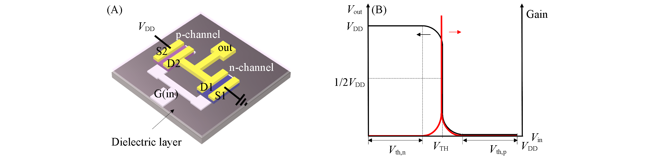
Fig.1 Structure of complementary inverter(A), transfer characteristic(black) and gain characteristic(red) of complementary inverter(B)S1: source electrode of n?channel FET; D1: drain electrode of n?channel FET; S2: source electrode of p?channel FET; D2: drain electrode of p?channel FET.
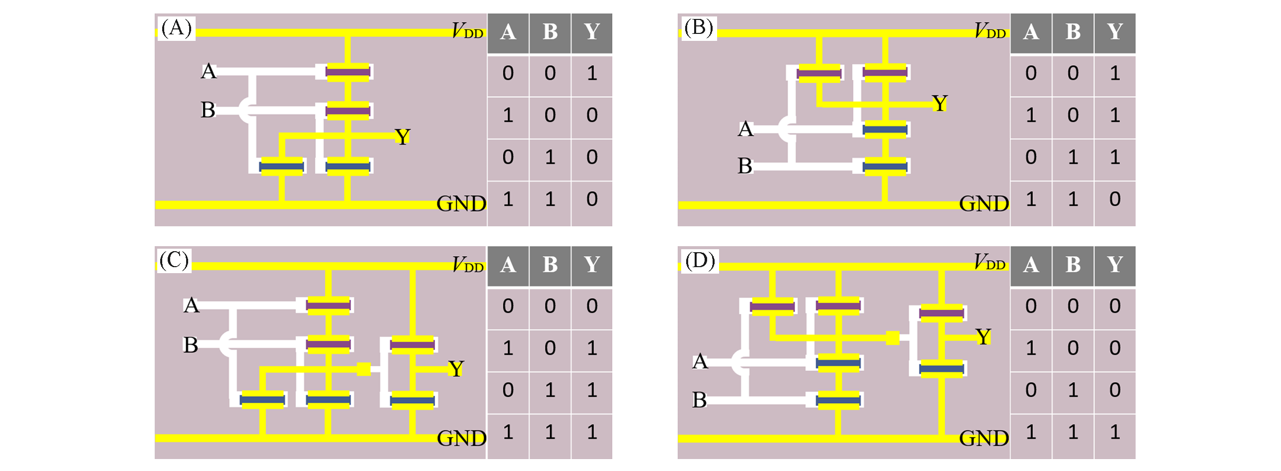
Fig.2 Gate structures and the truth tables of NOR(A), NAND(B), OR(C), and AND(D)VDD: Power source; GND: ground; A: input A; B: input B; Y: output; yellow parts: top electrodes; white parts: bottom electrodes; purple parts: p-channel semiconductor; blue parts: n-channel semiconductor.
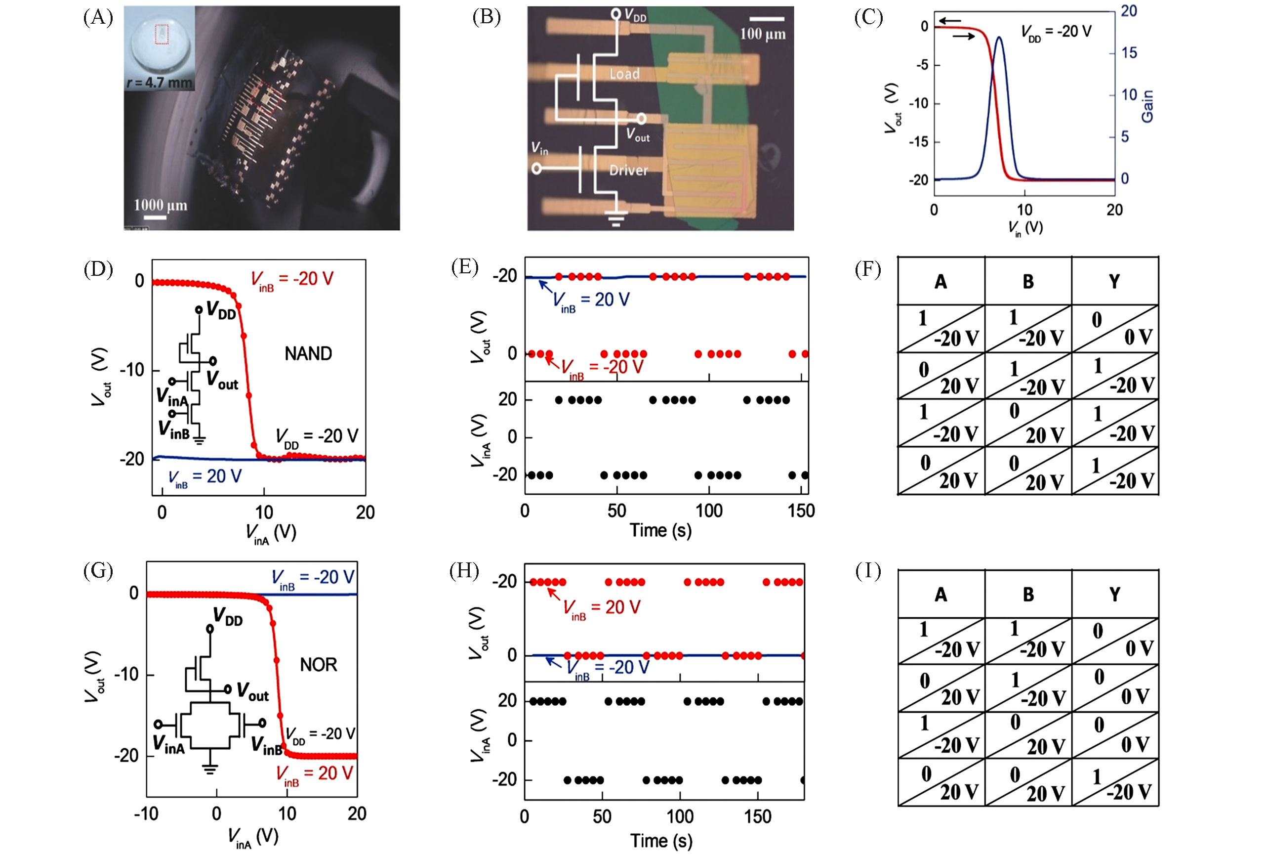
Fig.3 3D optical microscopy image(A), magnified optical image of an inverter(B), static voltage transfer characteristics and the corresponding signal gain of the inverter operated at VDD=-20 V(C), static voltage transfer characteristics at VDD=-20 V for NAND gate(D) and NOR gate(G), dynamic switching characteristics at VDD=-20 V for NAND gate(E) and NOR gate(H), logic truth tables for NAND gate(F) and NOR gate(I)[34]Insets of (D) and (G): the corresponding circuit diagrams. Copyright 2015, Wiley?VCH.
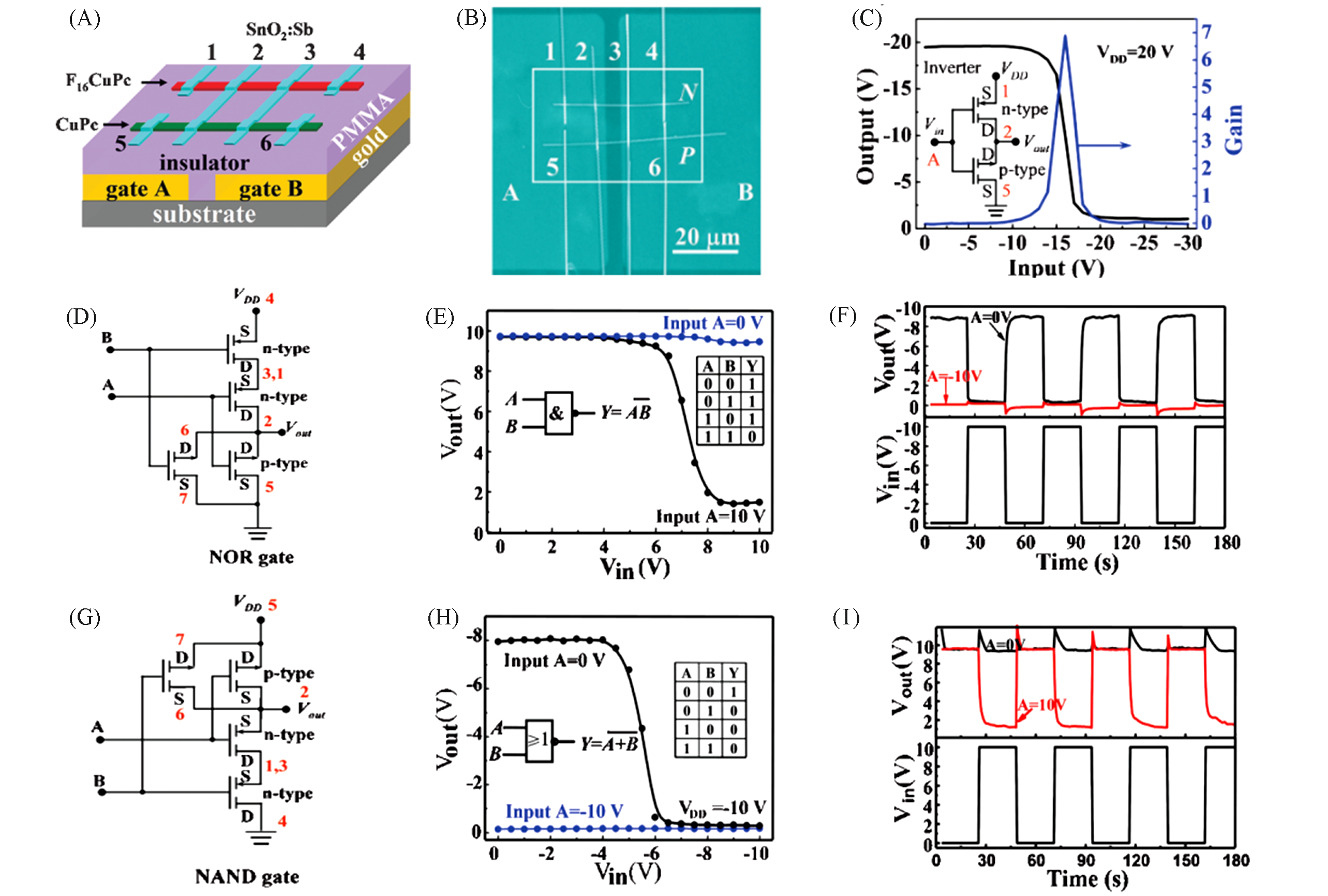
Fig.4 Schematic diagrams(A) and SEM image(B) of organic single crystal circuits assembled by using nanowires of CuPc, F16CuPc, and SnO2:Sb as building blocks, static voltage transfer characteristics and gain of an inverter at VDD=20 V(C), circuit schematic diagrams of NOR(D) and NAND(G) logic gates, transfer(E) and dynamic switching(F) characteristics of a NOR gate at VDD=10 V, transfer(H) and dynamic switching(I) characteristics of a NAND gate at VDD=10 V[39]Copyright 2009, Wiley?VCH.
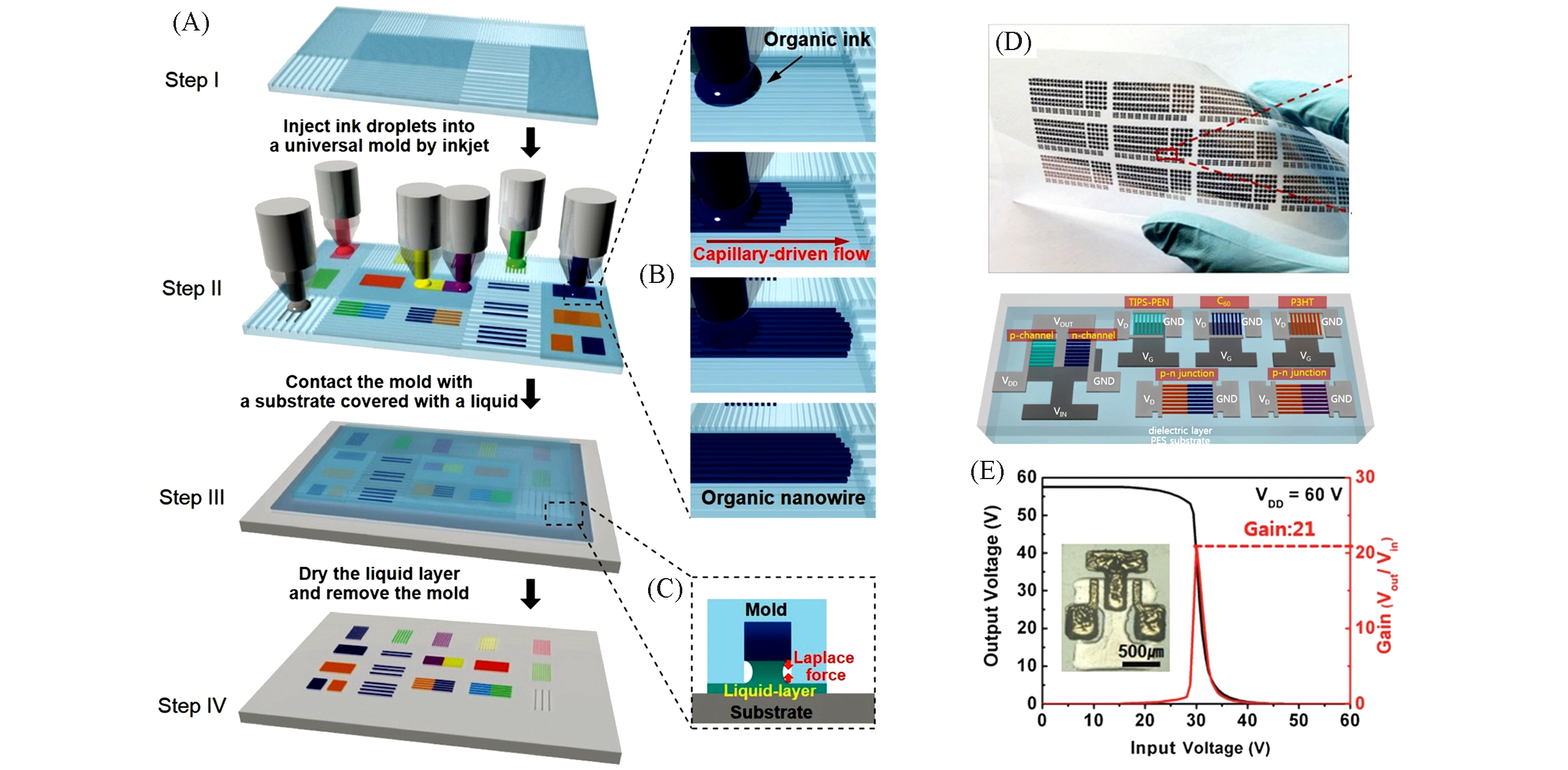
Fig.5 Schematic illustration of the inkjet?NTP process(A), schematic illustration of an ink droplet filling the recessed nanochannels of a selected area of the mold through capillary?driven flow(B), schematic illustration of a liquid bridge formed by a polar liquid layer between the nanowires and a substrate(C), a photographic image of the integrated electronic devices composed of FET, inverter, and p?n diode arrays made of single?crystal organic nanowires(D), static voltage transfer characteristics and signal gain of a representative inverter composed of TIPS?PEN and C60 FETs(E)[41]Copyright 2016, Wiley?VCH.
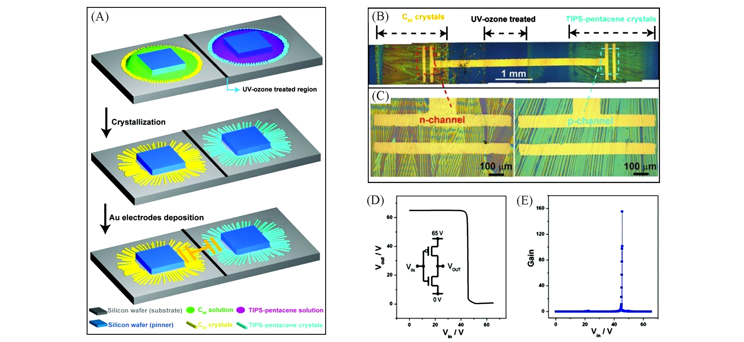
Fig.6 Schematic illustration of the DPC method and inverter fabricating process(A), a composite image from several optical microscopy(OM) images, showing the positioned regions of well?aligned C60 and TIPS?PEN crystals(B), the channels of the inverter(C), the static voltage transfer characteristics(D) and the corresponding gain of a inverter(E)[47]Inset of (D): the inverter circuit configuration. Copyright 2012, Wiley?VCH.
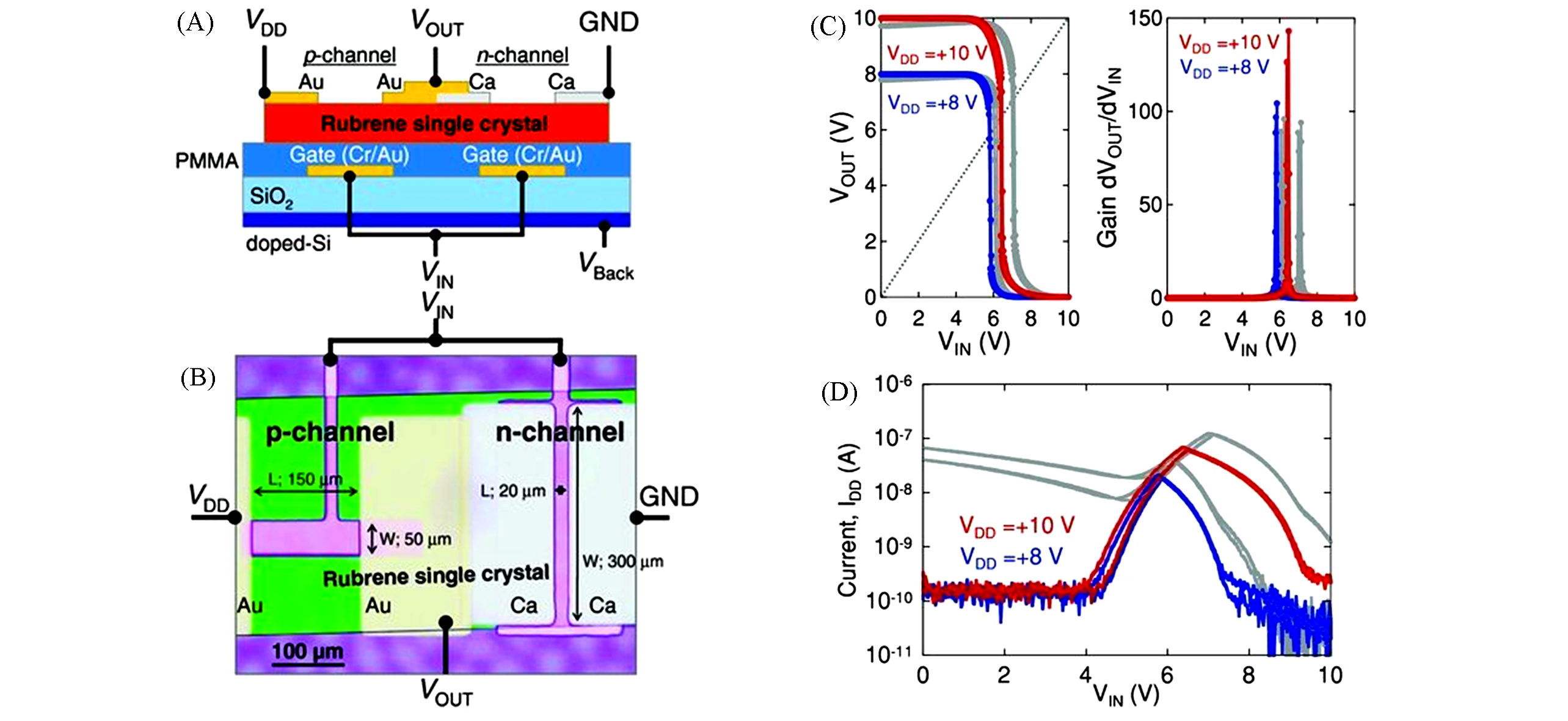
Fig.7 Schematic illustration of a monolithic complementary inverter using a rubrene single crystal(A), optical view of the typical device(B), voltage transfer characteristics of the inverter with applying a back gate voltage of +10 V(left), and corresponding DC values of inverter switching(right)(C), penetration current between the VDD and GND terminals at the switching(D)[48]Copyright 2010, Wiley?VCH.
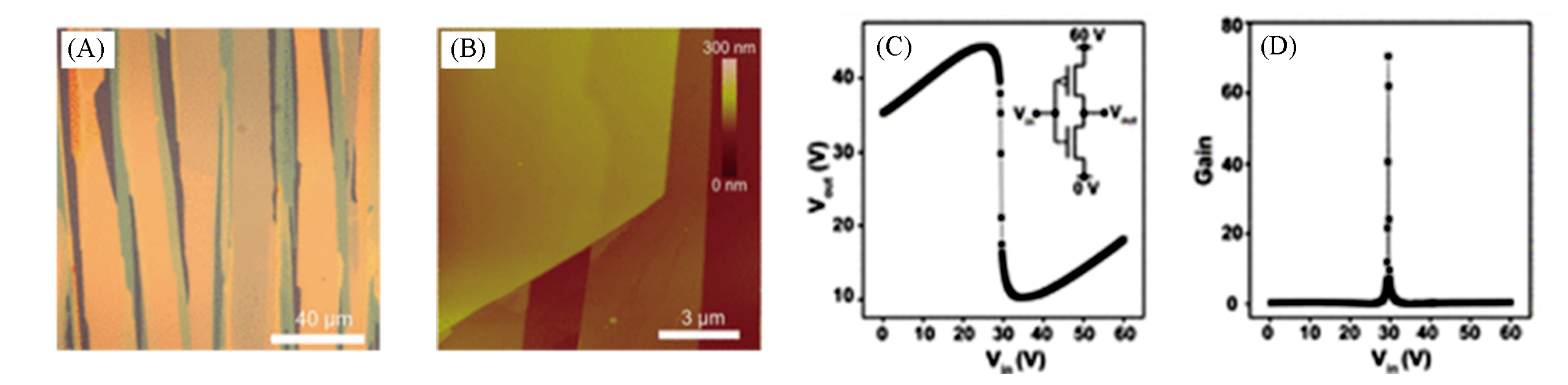
Fig.8 An OM image of the bilayer TIPS?TAP and TIPS?BP crystals, showing the bilayer structure with wide ribbons crystals(yellow) and narrow ones(blue)(A), an AFM image of bilayer structure showing the top layer as wide crystals and the bottom layers as narrow crystals(B), the voltage transfer characteristics(C) and corresponding gain of an inverter(D)[54]Inset of (C): the inverter configuration. Copyright 2019, American Chemical Society.
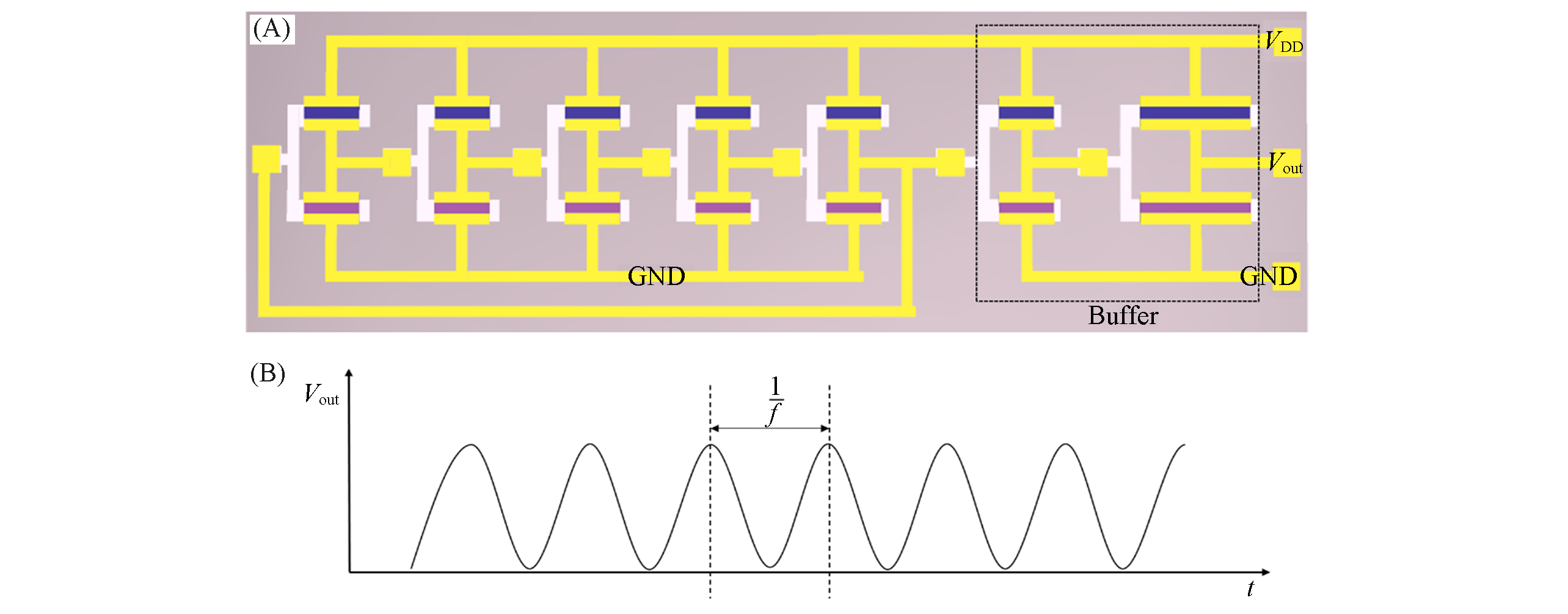
Fig.9 Schematic diagram(A) and output characteristic(B) of 5?stage ring oscillator
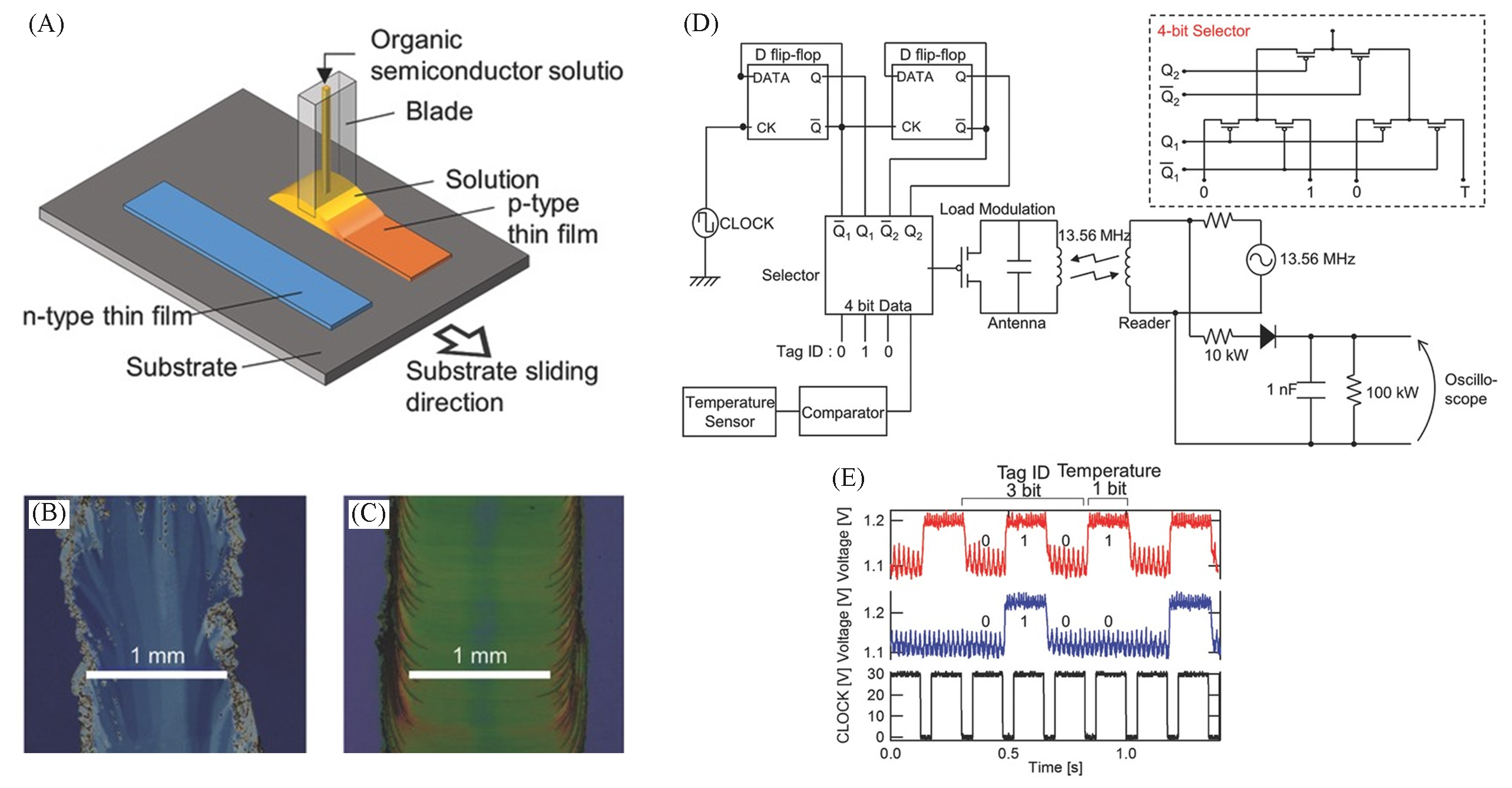
Fig.10 A diagram showing the present crystal growth method(A), photographic images of organic single crystalline films of p?type(B) and n?type(C) semiconductors, a schematic of the RFID prototype(left) and a circuit diagram of the 4?bit selector(right)(D) and the signal received at the reader oscilloscope at two different temperatures(E)(E) The top and middle signals show the output when the temperature is above and below 50 °C, respectively. The bottom signals represent the CLOCK[64]. Copyright 2017, Wiley?VCH.
| 1 | Crone B., Dodabalapur A., Lin Y. Y., Filas R. W., Bao Z., LaDuca A., Sarpeshkar R., Katz H. E., Li W., Nature, 2000, 403(6769), 521―523 |
| 2 | Deng W., Zhang X., Pan H., Shang Q., Wang J., Zhang X., Zhang X., Jie J., Sci. Rep., 2014, 4(i), 1―7 |
| 3 | Diao Y., Tee B. C. K., Giri G., Xu J., Kim D. H., Becerril H. A., Stoltenberg R. M., Lee T. H., Xue G., Mannsfeld S. C. B., Bao Z., Nat. Mater., 2013, 12(7), 665―671 |
| 4 | Zhang L., Wang H., Zhao Y., Guo Y., Hu W., Yu G., Liu Y., Adv. Mater., 2013, 25(38), 5455―5460 |
| 5 | Gelinck G. H., Huitema H. E. A., van Veenendaal E., Cantatore E., Schrijnemakers L., van Der Putten J. B. P. H., Geuns T. C. T., Beenhakkers M., Giesbers J. B., Huisman B. H., Meijer E. J., Benito E. M., Touwslager F. J., Marsman A. W., van Rens B. J. E., de Leeuw D. M., Nat. Mater., 2004, 3(2), 106―110 |
| 6 | Someya T., Sekitani T., Iba S., Kato Y., Kawaguchi H., Sakurai T., Whitesides G. M., Jul N., PNAS, 2004, 101, 9966―9970 |
| 7 | Someya T., Kato Y., Sekitani T., Kawaguchi H., IEEE Trans. Electron Devices, 2005, 52(11), 2502―2511 |
| 8 | Kato Y., Sekitani T., Noguchi Y., Yokota T., Takamiya M., Sakurai T., Someya T., IEEE Trans. Electron Devices, 2010, 57(5), 995―1002 |
| 9 | Cantatore E., Geuns T. C. T., Gruijthuijsen A. F. A., Gelinck G. H., Drews S., de Leeuw D. M., IEEE Int. Solid⁃State Circuits, 2006, 42(1), 84―92 |
| 10 | Myny K., Steudel S., Smout S., Vicca P., Furthner F., van der Putten B., Tripathi A. K., Gelinck G. H., Genoe J., Dehaene W., Heremans P., Org. Electron., 2010, 11(7), 1176―1179 |
| 11 | Karimov K. S., Qazi I., Khan T. A., Draper P. H., Khalid F. A., Mahroof⁃Tahir M., Environ. Monit. Assess., 2008, 141(1―3), 323―328 |
| 12 | Sekitani T., Yokota T., Zschieschang U., Klauk H., Bauer S., Takeuchi K., Takamiya M., Sakurai T., Someya T., Science, 2009, 326(5959), 1516―1519 |
| 13 | Bernards D. A., Malliaras G. G., Owens R. M., Organic Semiconductors in Sensor Applications, Springer⁃verlag, Berlin Heidelbeg, 2008, 263─278 |
| 14 | Podzorov V., Menard E., Borissov A., Kiryukhin V., Rogers J. A., Gershenson M. E., Phys. Rev. Lett., 2004, 93(8), 1―4 |
| 15 | Takahashi Y., Hasegawa T., Horiuchi S., Kumai R., Tokura Y., Saito G., Chem. Mater., 2007, 19(26), 6382―6384 |
| 16 | Butko V. Y., Chi X., Lang D. V, Ramirez A. P., Appl. Phys. Lett., 2003, 83(23), 4773―4775 |
| 17 | Wang A., Kymissis I., Bulovic V., Akinwande A. I., Appl. Phys. Lett., 2006, 89(11), 5812―5877 |
| 18 | Martínez Hardigree J. F., Katz H. E., Acc. Chem. Res., 2014, 47(4), 1369―1377 |
| 19 | Brown A. R., Pomp A., Hart C. M., de Leeuw D. M., Science, 1995, 270(5238), 972―974 |
| 20 | You A., Be M. A. Y., In I., Appl. Phys. Lett., 1998, 73(1), 108―110 |
| 21 | Sirringhaus A. H., Kawase T., Friend R. H., Shimoda T., Inbasekaran M., Wu W., Woo E. P., Science, 2000, 290(5499), 2123―2126 |
| 22 | Dodabalapur A., Laquindanum J., Katz H. E., Bao Z., Appl. Phys. Lett., 1996, 69(27), 4227―4229 |
| 23 | Lin Y. Y., Dodabalapur A., Sarpeshkar R., Bao Z., Li W., Baldwin K., Raju V. R., Katz H. E., Appl. Phys. Lett., 1999, 74(18), 2714―2716 |
| 24 | Na J. H., Kitamura M., Arakawa Y., Appl. Phys. Lett., 2008, 93(21), 1―4 |
| 25 | Roh J., Roh H., Shin H., Kim H., Lee C., Polym. Bull., 2016, 73(9), 2531―2537 |
| 26 | Ng T. N., Sambandan S., Lujan R., Arias A. C., Newman C. R., Yan H., Facchetti A., Appl. Phys. Lett., 2009, 94(23), 2007―2010 |
| 27 | Brown A. R., Jarrett C. P., de Leeuw D. M., Matters M., Synth. Met., 1997, 88(1), 37―55 |
| 28 | De Boer R. W. I., Stassen A. F., Craciun M. F., Mulder C. L., Molinari A., Rogge S., Morpurgo A. F., Appl. Phys. Lett., 2005, 86(262109), 1―3 |
| 29 | Sundar V. C., Zaumseil J., Podzorov V., Menard E., Willett R. L., Someya T., Gershenson M. E., Rogers J. A, Science, 2004, 303(5664), 1644―1646 |
| 30 | Jurchescu O. D., Popinciuc M., van Wees B. J., Palstra T. T. M., Adv. Mater., 2007, 19(5), 688―692 |
| 31 | Jiang H., Yang X., Cui Z., Liu Y., Li H., Hu W., Liu Y., Zhu D., Appl. Phys. Lett., 2007, 91(12), 123505 |
| 32 | Zeis R., Siegrist T., Kloc C., Appl. Phys. Lett., 2005, 86(2), 84―87 |
| 33 | Jiang L., Hu W., Wei Z., Xu W., Meng H., Adv. Mater., 2009, 21(36), 3649―3653 |
| 34 | Zhao X., Tong Y., Tang Q., Liu Y., Adv. Electron. Mater., 2015, 1(12), 1―10 |
| 35 | Kang J., Lee M., Facchetti A., Kim J., Park S. K., RSC Adv., 2018, 8(31), 17417―17420 |
| 36 | Larsen C., Wang J., Edman L., Thin Solid Films, 2012, 520(7), 3009―3012 |
| 37 | Min S. Y., Kim T. S., Kim B. J., Cho H., Noh Y. Y., Yang H., Cho J. H., Lee T. W., Nat. Commun., 2013, 4, 1―9 |
| 38 | Briseno A. L., Tseng R. J., Li S. H., Chu C. W., Yang Y., Falcao E. H. L., Wudl F., Ling M. M., Chen H. Z., Bao Z., Meng H., Kloc C., Appl. Phys. Lett., 2006, 89(22), 1―4 |
| 39 | Tang Q., Tong Y., Hu W., Wan Q., Bjørnholm T., Adv. Mater., 2009, 21(42), 4234―4237 |
| 40 | Park K. S., Cho B., Baek J., Hwang J. K., Lee H., Sung M. M., Adv. Funct. Mater., 2013, 23(38), 4776―4784 |
| 41 | Park K. S., Baek J., Park Y., Lee L., Lee Y. E. K., Kang Y., Sung M. M., Adv. Mater., 2016, 28(15), 2874―2880 |
| 42 | Zheng S., Xiong X., Zheng Z., Xu T., Zhang L., Zhai T., Lu X., Carbon, 2018, 126, 299―304 |
| 43 | Peng B., Wang Z., Chan P. K. L., J. Mater. Chem. C, 2016, 4(37), 8628―8633 |
| 44 | Li H., Tee B. C. K., Cha J. J., Cui Y., Chung J. W., Lee S. Y., Bao Z., J. Am. Chem. Soc., 2012, 134(5), 2760―2765 |
| 45 | Li H., Fan C., Vosgueritchian M., Tee B. C. K., Chen H., J. Mater. Chem. C, 2014, 2(18), 3617―3624 |
| 46 | Wu J., Fan C., Xue G., Ye T., Liu S., Lin R., Chen H., Xin H. L., Xiong R. G., Li H., Adv. Mater., 2015, 27(30), 4476―4480 |
| 47 | Li H., Tee B. C. K., Giri G., Chung J. W., Lee S. Y., Bao Z., Adv. Mater., 2012, 24(19), 2588―2591 |
| 48 | Uemura T., Yamagishi M., Okada Y., Nakayama K., Yoshizumi M., Uno M., Takeya J., Adv. Mater., 2010, 22(35), 3938―3941 |
| 49 | Anthopoulos T. D., de Leeuw D. M., Cantatore E., Setayesh S., Meijer E. J., Tanase C., Hummelen J. C., Blom P. W. M., Appl. Phys. Lett., 2004, 85(18), 4205―4207 |
| 50 | Anthopoulos T. D., Setayesh S., Smits E., Cölle M., Cantatore E., de Boer B., Blom P. W. M., de Leeuw D. M., Adv. Mater., 2006, 18(14), 1900―1904 |
| 51 | Xue G., Fan C., Wu J., Liu S., Liu Y., Chen H., Xin H. L., Li H., Mater. Horizons, 2015, 2(3), 344―349 |
| 52 | Fan C., Zoombelt A. P., Jiang H., Fu W., Wu J., Yuan W., Wang Y., Li H., Chen H., Bao Z., Adv. Mater., 2013, 25(40), 5762―5766 |
| 53 | Li H., Fan C., Fu W., Xin H. L., Chen H., Angew. Chem.⁃Int. Ed., 2015, 54(3), 956―960 |
| 54 | Li H., Wu J., Takahashi K., Ren J., Wu R., Cai H., Wang J., Xin H. L., Miao Q., Yamada H., Chen H., Li H., J. Am. Chem. Soc., 2019, 141(25), 10007―10015 |
| 55 | Meijer E. J., de Leeuw D. M., Setayesh S., van Veenendaal E., Huisman B. H., Blom P. W. M., Hummelen J. C., Scherf U., Klapwijk T. M., Nat. Mater., 2003, 2(10), 678―682 |
| 56 | Park W. T., Kang S. J., Noh Y. Y., Mol. Cryst. Liq. Cryst., 2014, 600(1), 123―128 |
| 57 | Kim F. S., Guo X., Watson M. D., Jenekhe S. A., Adv. Mater., 2010, 22(4), 478―482 |
| 58 | Watson C. P., Brown B. A., Carter J., Morgan J., Taylor D. M., Adv. Electron. Mater., 2016, 2(3), 1500322 |
| 59 | Herlogsson L., Cölle M., Tierney S., Crispin X., Berggren M., Adv. Mater., 2010, 22(1), 72―76 |
| 60 | Yoo B., Jung T., Basu D., Dodabalapur A., Jones B. A., Facchetti A., Wasielewski M. R., Marks T. J., Appl. Phys. Lett., 2006, 88, 082104 |
| 61 | Kraft U., Sejfić M., Kang M. J., Takimiya K., Zaki T., Letzkus F., Burghartz J. N., Weber E., Klauk H., Adv. Mater., 2015, 27(2), 207―214 |
| 62 | Kempa H., Hambsch M., Reuter K., Stanel M., Schmidt G. C., Meier B., Hübler A. C., IEEE Trans. Electron Devices, 2011, 58(8), 2765―2769 |
| 63 | Cai X., Ji D., Jiang L., Zhao G., Tan J., Tian G., Li J., Hu W., Appl. Phys. Lett., 2014, 104(6), 063305 |
| 64 | Yamamura A., Matsui H., Uno M., Isahaya N., Tanaka Y., Kudo M., Ito M., Mitsui C., Okamoto T., Takeya J., Adv. Electron. Mater., 2017, 3(7), 1―6 |
| 65 | Kato Y., Iba S., Teramoto R., Sekitani T., Someya T., Kawaguchi H., Sakurai T., Appl. Phys. Lett., 2004, 84(19), 3789―3791 |
| 66 | Kalb W. L., Mathis T., Haas S., Stassen A. F., Batlogg B., Appl. Phys. Lett., 2007, 90, 092104 |
| 67 | Walser M. P., Kalb W. L., Mathis T., Brenner T. J., Batlogg B., Appl. Phys. Lett., 2009, 94, 053303 |
| 68 | Jung S., Albariqi M., Gruntz G., Al⁃Hathal T., Peinado A., Garcia⁃Caurel E., Nicolas Y., Toupance T., Bonnassieux Y., Horowitz G., ACS Appl. Mater. Interfaces, 2016, 8(23), 14701―14708 |
| 69 | Kato Y., Sekitani T., Takamiya M., Doi M., Asaka K., Sakurai T., Someya T., IEEE Trans. Electron Devices, 2007, 54(2), 202―209 |
| 70 | Sekitani T., Takamiya M., Noguchi Y., Nakano S., Kato Y., Sakurai T., Someya T., Nat. Mater., 2007, 6(6), 413―417 |
| 71 | Kondo M., Uemura T., Matsumoto T., Araki T., Yoshimoto S., Sekitani T., Appl. Phys. Express, 2016, 9(6), 1―4 |
| 72 | Kim D. H., Ahn J. H., Kim H. S., Lee K. J., Kim T. H., Yu C. J., Nuzzo R. G., Rogers J. A., IEEE Electron Device Lett., 2008, 29(1), 73―76 |
| [1] | 王剑桥, 马於光. 有机半导体非平衡态HOMO和LUMO能量位移规律与OLED中“热激子”形成的唯象理解[J]. 高等学校化学学报, 2022, 43(4): 20210856. |
| [2] | 朱磊, 韩军燕, 常海珍, 邱宇渊, 张雅楠, 彭丹妮, 胡伟, MiaoShaobin. 二胺与二酮环聚合反应的不同途径与产物[J]. 高等学校化学学报, 2018, 39(12): 2686. |
| [3] | 陈九菊. 有机半导体Terazulene单晶双极电荷传输性质的理论研究[J]. 高等学校化学学报, 2016, 37(1): 121. |
| [4] | 田洪坤,史建武,闫东航,王利祥,耿延候,王佛松 . 2,5-二(2-菲基)-[3,2-b]并二噻吩的合成、表征及在有机薄膜晶体管中的应用[J]. 高等学校化学学报, 2006, 27(9): 1677. |
| [5] | 侯小珂, 杜锡光, 马春雨, 李燕, 张清林, 王旭, 常玉春, 姜文海, 单士军, 姜秀英, 杜国同. 外围缩合四个1,10-啡啰啉单元的新氮杂酞菁的表面光伏响应及电场作用研究[J]. 高等学校化学学报, 2005, 26(7): 1294. |
| [6] | 周雪琴, 汪茫, 杨士林. 有机半导体材料中的电荷转移[J]. 高等学校化学学报, 2000, 21(8): 1312. |
| 阅读次数 | ||||||
|
全文 |
|
|||||
|
摘要 |
|
|||||