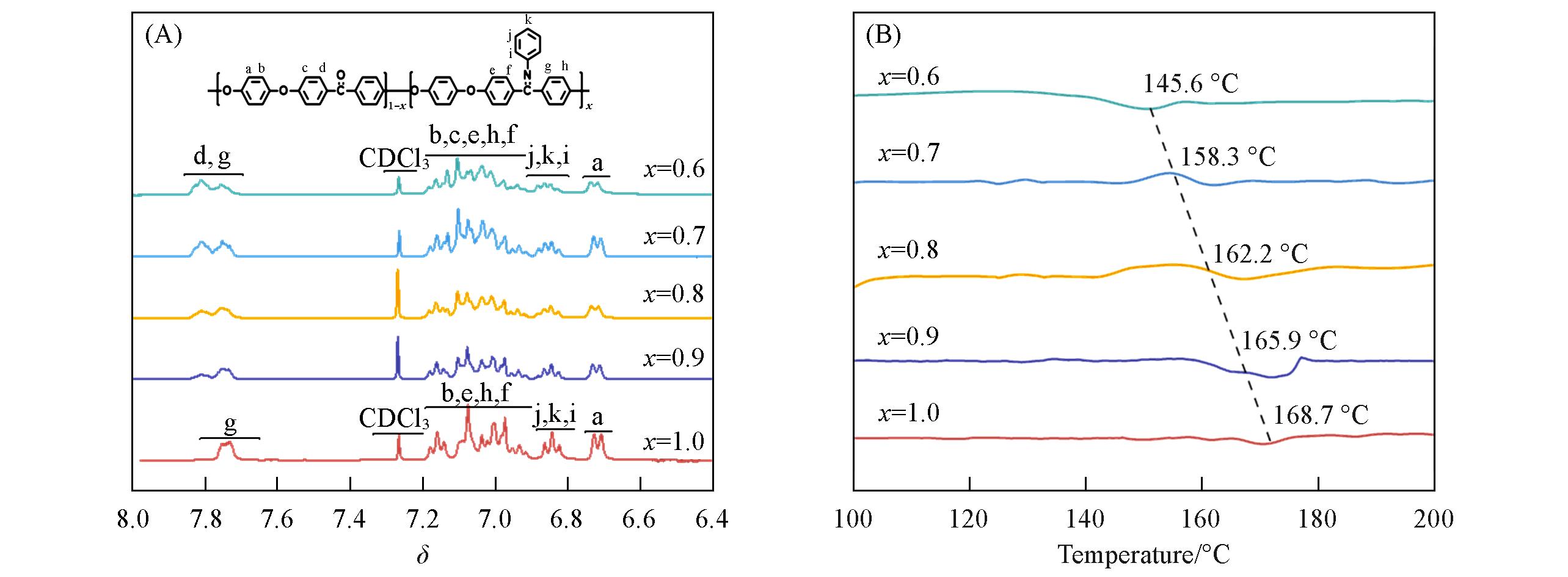
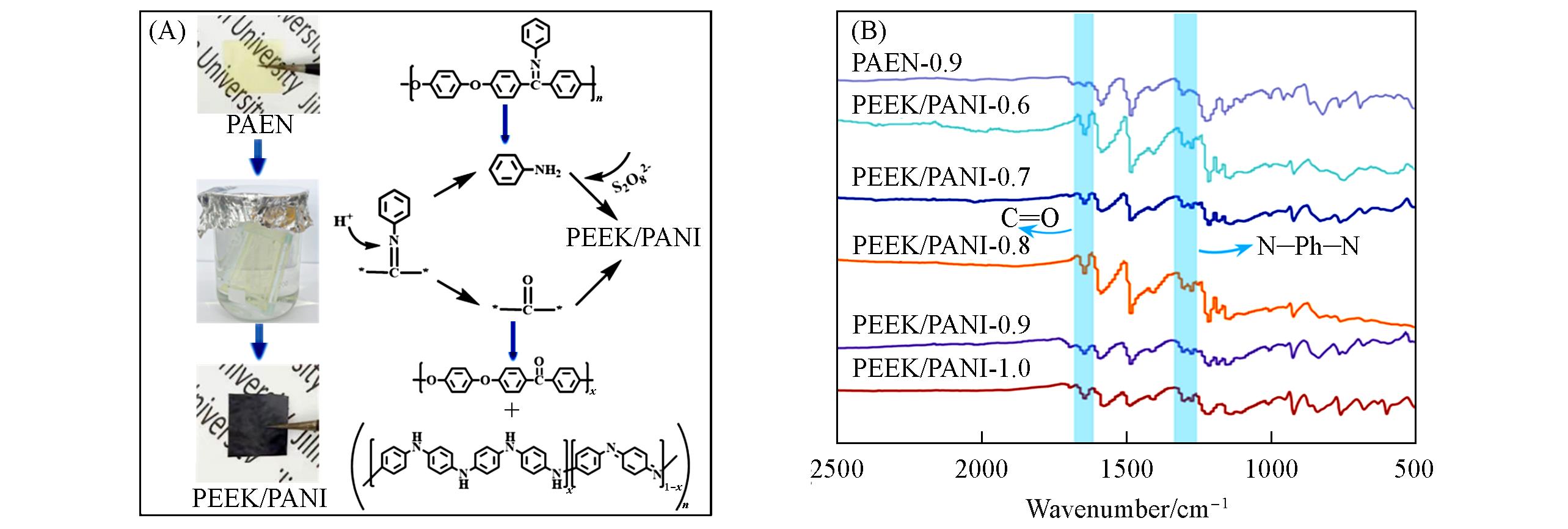
| [11] |
Peng X. D., Wang Y. M., Huang X., Li K., Hydraul. Pneum. Seals, 2009, 29(4), 4—11
|
|
彭旭东, 王玉明, 黄兴, 李鲲. 液压气动与密封, 2009, 29(4), 4—11
|
| [12] |
Qin Y., Yi J. N., Wu Y. Q., Wu Q. L., Zhang Z., Li L., Sci. Silvae. Sin., 2018, 54(3), 134—143
|
|
卿彦, 易佳楠, 吴义强, 吴清林, 张振, 李蕾. 林业科学, 2018, 54(3), 134—143
|
| [13] |
Hou L. L., Zhang M. L., Lang F. X., Zheng X. Y., Liu L. M., Chem. Ind. Eng. Prog., 2024, 43(10), 5837—5856
|
|
候林丽, 张梦玲, 郎锋样, 郑希怡, 刘利民. 化工进展, 2024, 43(10), 5837—5856
|
| [14] |
Zhao Y. F., Mater. China, 2013, 32(4), 217—242
|
|
赵云峰. 中国材料进展, 2013, 32(4), 217—242
|
| [15] |
Liu L., Zhang D., J. Funct. Mater., 2015, 46(3), 3016—3022
|
|
刘琳, 张东. 功能材料, 2015, 46(3), 3016—3022
|
| [16] |
Song Y. X., Wei Y., Zheng Y. S., Xu C. R., N. Chem. Mater., 2000, 28(9), 3—7
|
|
宋月贤, 韦玮, 郑元锁, 徐传镶. 化工新型材料, 2000, 28(9), 3—7
|
| [17] |
Zhao X., Qiu P. D., Jiang H. J., Jin Z. X., Cai K. D., Electron. Compon. Mater., 2015, 34(1), 1—8
|
|
赵雪, 邱平达, 姜海静, 金振兴, 蔡克迪. 电子元件与材料, 2015, 34(1), 1—8
|
| [18] |
Zhang X. M., Yang K., Jiao M. L., Diao Q., Zhu G. X., Jia W. S., Cao J., Shanghai Text. Sci. Technol., 2020, 48(8), 17—21
|
|
张啸梅, 杨凯, 焦明立, 刁泉, 朱根兴, 贾万顺, 曹健. 上海纺织科技, 2020, 48(8), 17—21
|
| [19] |
Karami H., Mousavi M. F., Shamsipur M., J. Power Sources, 2003, 117(1/2), 255—259
|
| [20] |
Wang G., Morrin A., Li M., Liu N., Luo X., J. Mater. Chem. B, 2018, 6(25), 4173—4190
|
| [21] |
Yang Y., Qiang J. F., Jing X. L., Yao S., N. Chem. Mater., 2003, 31(3), 1—6
|
|
杨勇, 强军锋, 井新利, 姚胜. 化工新型材料, 2003, 31(3), 1—6
|
| [22] |
Mao C. Y., Zhao S., He P. P., Wang Z., Wang J. X., Chem. Eng. J., 2021, 414, 128929
|
| [23] |
Amura I. F., Shahid S., Sarihan A., Shen J., Patterson D. A., Emanuelsson E. A. C., J. Membr. Sci., 2021, 620, 117712
|
| [24] |
Rayar A., Prasanna G. D., Shreedhara K. M., Dobbidi P., Rekha Phani P. S. D., Naveen C. S., Synth. Metals, 2026, 317, 118023
|
| [25] |
Mohajer S., Dorraj M. S. S., Rasoulifard M. H., Hajimiri I., ACS Appl. Polym. Mater., 2025, 7, 15394—15407
|
| [26] |
Zhou L., Meng Z. T., Sun B., Xue C. F., Xu B. F., Gu L. L., N. Chem. Mater., 2025, 53(Suppl. 1), 63—75
|
| [1] |
Wu H., Yu G., Pan L., Liu N., McDowell M. T., Bao Z., Cui Y., Nat. Commun., 2013, 4, 1943
|
| [2] |
Santoro M., Gorelli F. A., Bini R., Haines J., van der Lee A., Nat. Commun., 2013, 4, 1557
|
| [3] |
Wang Y., Zanelotti C. J., Wang X., Kerr R., Jin L., Kan W. H., Dingemans T. J., Forsyth M., Madsen L. A., Nat. Mater., 2021, 20(9), 1255—1263
|
| [4] |
Orava J., Balachandran S., Han X., Shuleshova O., Nurouzi E., Soldatov I., Oswald S., Gutowski O., Ivashko O., Dippel A. C., Zimmermann M. V., Ivanov Y. P., Greer A. L., Raabe D., Herbig M., Kaban I., Nat. Commun., 2021, 12(1), 2839
|
| [5] |
Chung H. T., Won J. H., Zelenay P., Nat. Commun., 2013, 4, 1922
|
| [6] |
Lin Z., Cao N., Sun Z., Li W., Sun Y., Zhang H., Pang J., Jiang Z., Adv. Sci., 2022, 9(1), e2103706
|
| [7] |
Chen M. X., Wang X. Y., Zhang W., Xiao C. F., Chem. Ind. Eng. Prog., 2023, 42(5), 2439—2453
|
|
陈明星, 王新亚, 张威, 肖长发. 化工进展, 2023, 42(5), 2439—2453
|
| [8] |
Ding S. J., Zhao Y. Z., Ge D. B., Mater. Rep., 2008, 22(4), 30—37
|
|
丁世敬, 赵跃智, 葛德彪. 材料导报, 2008, 22(4), 30—37
|
| [9] |
Chen S. J., Acta Aeronaut. Astronaut. Sin., 2008, 29(3), 605—610
|
|
陈绍杰. 航空学报, 2008, 29(3), 605—610
|
| [10] |
Lin N., Lin Z. R., Chen H. N., Lu L. S., J. Mech. Eng., 2022, 58(3), 235—250
|
| [26] |
周文, 孟照婷, 孙彬, 薛超凡, 许宝方, 顾璐璐. 化工新型材料, 2025, 53(Suppl. 1), 63—75
|
| [27] |
Xu Z. H., Yi H., Fang T., Liu J. S., Wang Y. S., Tan X. M., Gui T. J., J. Qingdao Univ. Technol., 2025, 46(4), 109—116
|
|
徐振华, 尹红, 方涛, 刘杰胜, 王源升, 谭晓明, 桂泰江. 青岛理工大学学报, 2025, 46(4), 109—116
|
| [28] |
Zhang K. J., Tech. Text., 2025, 43(7), 39—46
|
|
张坤杰. 产业用纺织品, 2025, 43(7), 39—46
|
| [29] |
Cao N., Yue C., Lin Z., Li W., Zhang H., Pang J., Jiang Z., J. Hazard. Mater., 2021, 414, 125489
|
| [10] |
蔺娜, 林志燃, 陈瀚宁, 陆龙生. 机械工程学报, 2022, 58(3), 235—250
|
 )
)